Nand gate Vhdl tutorial – 5: design, simulate and verify nand, nor, xor and xnor Inverter gate symbol
[DIAGRAM] Circuit Diagram Nand Gate - MYDIAGRAM.ONLINE
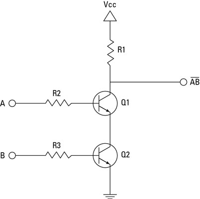
Nand logic gate circuit diagram
Nand gate circuit diagram using diode iot wiring diagram 19152
[diagram] circuit diagram nand gateNand gate circuit diagram and working explanation Nand gate diagram[diagram] logic diagram using nand gate.
Conversion of nand gate to basic gatesNand gates nor xnor circuit vhdl xor logic verify simulate truth circuits tutorial basic ckt Nand gate circuit diagram using transistor2 input nand gate circuit diagram.

Nand logic gate circuit diagram
Nand gate truth tableDigital logic Nand gate circuit diagram inputs input electronic through pull down explanation working circuits button connected then powerXor gate circuit diagram.
Nand gates componentsNand gate ic 7400 structure internal nor numbering go back quad component ics show Introduction to logic gatesNand gate circuit diagram and working explanation.

Debouncing circuit using nand gate
Nand gate diagramNand gates logic using nor gate only input circuit truth table various Circuit diagram of nand logic gateVhdl tutorial – 5: design, simulate and verify nand, nor, xor and xnor.
[diagram] circuit diagram nand gate[diagram] logic diagram using nand gate Logic nand gate tutorial with nand gate truth tableXor nand logic nor gates xnor circuit vhdl simulate verify truth input circuits tutorial engineersgarage inverter scosche inputs ckt combined.
![[DIAGRAM] Logic Diagram Using Nand Gate - MYDIAGRAM.ONLINE](https://i2.wp.com/qph.fs.quoracdn.net/main-qimg-95aed35418efab2177182c1c5896f710)
Circuit diagram of nand logic gate
Nand gate logic diagram .
.

![[DIAGRAM] Circuit Diagram Nand Gate - MYDIAGRAM.ONLINE](https://i2.wp.com/www.researchgate.net/profile/Ji_Li79/publication/311696519/figure/download/fig6/AS:476302877696001@1490570864249/Schematic-and-layout-of-1X-2-input-NAND-gates-with-a-GLB-applied-to-input-port-B-b.png)


![[DIAGRAM] Circuit Diagram Nand Gate - MYDIAGRAM.ONLINE](https://i.ytimg.com/vi/DsPet6URykQ/maxresdefault.jpg)


![[DIAGRAM] Logic Diagram Using Nand Gate - MYDIAGRAM.ONLINE](https://i2.wp.com/www.allaboutcircuits.com/uploads/articles/pinout-diagram-for-4011-quad-NAND-gate.jpg)